Technical Documents
Specifications
Brand
FTDI ChipProgrammable Logic Technology
FPGA
Product Type
Programmable Logic Development Kit
Kit Classification
Module
For Use With
DAC121S101
Kit Name
Altera Cyclone-II
Standards/Approvals
RoHS
Country of Origin
China
Product Details
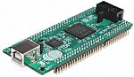
The Morph-IC-II is a USB based FPGA development module featuring the Altera Cyclone-II FPGA with the FTDI FT2232H USB to UART/FIFO/MPSSE converter IC. The module provides integration of Hi-Speed USB capability (480Mbit/s) with an FPGA, to enable ultra-fast software based FPGA configuration/reconfiguration and communication using the FTDI royalty free drivers.
An FPGA is a semiconductor device consisting of a matrix of Configurable Logic Blocks (CLBs) connected through programmable interconnects. The user determines these interconnections by programming SRAM. A CLB can be simple (AND, OR gates, etc) or complex (a block of RAM). The FPGA allows changes to be made to a design even after the device is soldered into a PCB.
VHDL reference designs, software samples and utilities
Stock information temporarily unavailable.
AED 540.62
AED 540.62 Each (ex VAT)
AED 567.65
AED 567.65 Each (inc. VAT)
1
AED 540.62
AED 540.62 Each (ex VAT)
AED 567.65
AED 567.65 Each (inc. VAT)
Stock information temporarily unavailable.
1
Technical Documents
Specifications
Brand
FTDI ChipProgrammable Logic Technology
FPGA
Product Type
Programmable Logic Development Kit
Kit Classification
Module
For Use With
DAC121S101
Kit Name
Altera Cyclone-II
Standards/Approvals
RoHS
Country of Origin
China
Product Details
The Morph-IC-II is a USB based FPGA development module featuring the Altera Cyclone-II FPGA with the FTDI FT2232H USB to UART/FIFO/MPSSE converter IC. The module provides integration of Hi-Speed USB capability (480Mbit/s) with an FPGA, to enable ultra-fast software based FPGA configuration/reconfiguration and communication using the FTDI royalty free drivers.
An FPGA is a semiconductor device consisting of a matrix of Configurable Logic Blocks (CLBs) connected through programmable interconnects. The user determines these interconnections by programming SRAM. A CLB can be simple (AND, OR gates, etc) or complex (a block of RAM). The FPGA allows changes to be made to a design even after the device is soldered into a PCB.
VHDL reference designs, software samples and utilities