Technical Documents
Specifications
Brand
Renesas ElectronicsProduct Type
Buffer/Clock Driver
Mount Type
Surface
Package Type
SSOP
Minimum Supply Voltage
3V
Pin Count
20
Maximum Supply Voltage
3.6V
Minimum Operating Temperature
-40°C
Maximum Operating Temperature
85°C
Standards/Approvals
No
Series
49FCT
Automotive Standard
No
Product Details
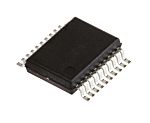
The Renesas Electronics buffer/non-inverting clock driver built using advanced dual metal CMOS technology. The device consists of two banks of drivers, each with a 1:5 fanout and its own output enable control. The device has a heartbeat monitor for diagnostics and PLL driving. The MON output is identical to all other outputs and complies with the output specifications in this document. It offers low capacitance inputs with hysteresis. It is designed for high speed clock distribution where signal quality and skew are critical. It is also allows single point-topoint transmission line driving in applications such as address distribution, where one signal must be distributed to multiple recievers with low skew and high signal quality.

Ideate. Create. Collaborate
JOIN FOR FREE
No hidden fees!


Stock information temporarily unavailable.
AED 318.43
AED 4.976 Each (In a Tube of 64) (ex VAT)
AED 334.35
AED 5.225 Each (In a Tube of 64) (inc. VAT)
64
AED 318.43
AED 4.976 Each (In a Tube of 64) (ex VAT)
AED 334.35
AED 5.225 Each (In a Tube of 64) (inc. VAT)
Stock information temporarily unavailable.
64
| Quantity | Unit price | Per Tube |
|---|---|---|
| 64 - 64 | AED 4.976 | AED 318.43 |
| 128 - 192 | AED 4.12 | AED 263.65 |
| 256 - 448 | AED 3.798 | AED 243.10 |
| 512 - 960 | AED 3.37 | AED 215.71 |
| 1024+ | AED 2.728 | AED 174.62 |
Ideate. Create. Collaborate
JOIN FOR FREE
No hidden fees!
Technical Documents
Specifications
Brand
Renesas ElectronicsProduct Type
Buffer/Clock Driver
Mount Type
Surface
Package Type
SSOP
Minimum Supply Voltage
3V
Pin Count
20
Maximum Supply Voltage
3.6V
Minimum Operating Temperature
-40°C
Maximum Operating Temperature
85°C
Standards/Approvals
No
Series
49FCT
Automotive Standard
No
Product Details
The Renesas Electronics buffer/non-inverting clock driver built using advanced dual metal CMOS technology. The device consists of two banks of drivers, each with a 1:5 fanout and its own output enable control. The device has a heartbeat monitor for diagnostics and PLL driving. The MON output is identical to all other outputs and complies with the output specifications in this document. It offers low capacitance inputs with hysteresis. It is designed for high speed clock distribution where signal quality and skew are critical. It is also allows single point-topoint transmission line driving in applications such as address distribution, where one signal must be distributed to multiple recievers with low skew and high signal quality.
Ideate. Create. Collaborate
JOIN FOR FREE
No hidden fees!